
Microelectronics has affected almost every walk of life such as healthcare and environment, education, agriculture, communication, robotics, automation, avionics, automobiles, instrumentation, power, military etc. Microelectronics is the key driver for the economic growth in its role as a technology driver, enabler and indicator of technological progress in the whole electronics chain. The phenomenal growth of the microelectronics technology has significantly contributed to the success of information and telecommunication technology in the last few decades.
Recognizing importance of microelectronics as the major economic contributor in the growth of the country, MeitY initiated the Microelectronics Development Programme in 1980s. The thrust of Microelectronics Development Programme has been to establish microelectronics base in the country through setting up of centres of excellence, technology development & capacity building through sponsored R&D projects in the area of Microelectronics. As a step towards the same, besides sponsoring other R&D projects in the area of Microelectronics, Centres for Analog Mixed Signal (AMS) Design for Design, Testing and Characterization were supported at IIT Madras, IISc Bangalore and CEERI Pilani. Also, with a view to make available industry-ready manpower specialized in VLSI design, Special Manpower Development Programme (SMDP) in VLSI Design was initiated earlier in three phases which resulted in increasing India’s share in the global VLSI Design market along with generation of 9300 and 38000 and 75000 specialized manpower in VLSI design area respectively.
Chips to Startup (C2S) Programme was initiated to train 85,000 number of Specialized Manpower at B.Tech, M.Tech & PhD Level over a period of 5 years in the area of VLSI and Embedded System Design and leapfrog in ESDM space by way of inculcating the culture of Chip/ System-on-Chip (SoC)/ System Level Design at Bachelors, Masters and Research level and act as a catalyst for growth of Start-ups involved in semiconductor design in the country.
Design Linked Incentive (DLI) Scheme was announced to offset the disabilities in the domestic industry involved in semiconductor design in order to not only move up in value-chain but also strengthen the semiconductor chip design ecosystem in the country. The Design Linked Incentive (DLI) Scheme aims to offer financial incentives as well as design infrastructure support across various stages of development and deployment of semiconductor design(s) for Integrated Circuits (ICs), Chipsets, System on Chips (SoCs), Systems & IP Cores and semiconductor linked design(s) over a period of 5 years to start-ups, MSMEs and domestic companies.
Projects for development of technologies/ products for societal, industrial and strategic sectors have also been initiated which include projects for design and development of Microprocessor, NavIC (Navigation with Indian Constellation) Receivers, Bluetooth Transceiver etc which not only aim to develop the technology base in the country in these areas but also to enable taking of complex designs in the country in the area of Microelectronics.
Broad Functions of Microelectronics:
- To establish microelectronics base in the country through setting up of Centres of Excellence, technology development & capacity building through sponsored R&D projects in the area of Microelectronics.
- Development of Indigenous technologies/products for societal, industrial and strategic sectors in the area of Microelectronics.
- To create vibrant semiconductor Chip Design ecosystem in the country by way of supporting fabless organizations for development of semiconductor products.
- Strengthen design infrastructure at incubators/ CoEs for fabless design and facilitate access to semiconductor design organizations.
- Achieve significant indigenization in semiconductor products and IPs deployed in the country, thereby facilitating import substitution and value addition in strategic, social & financial sectors.
Broad Thrust Areas of Microelectronics:
The following are the broad thrust area identified under Microelectronics Development programme:
- Translational research, import substitution & value addition in overall Electronics System Design value chain
- Capacity building in Microelectronics & related areas
- Fabless chip design for Automobiles, Mobility, Computing, Connectivity, Networking and Others areas (IoT/ Edge Devices etc)
- Discrete (Diode, Transistors etc) & Power Devices (IGBT, SiC devices, power supply control IC, power MOSFETs etc)
- Micro sensors, Detectors and Integrated MEMS
- Embedded System Design, EDA tools and related Software
- Hardware solutions for Positioning, Navigation, & Timing and AL/ ML
- Reusable Semiconductor IP Cores
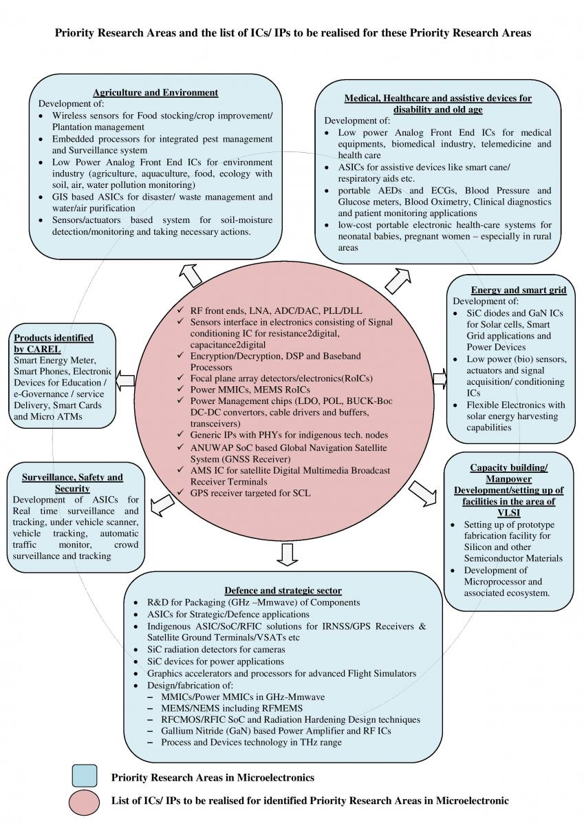
The Priority research areas identified for this year are:
For further information please contact:
Smt. SunitaVerma
Scientist ‘G’ & Group Coordinator (R&D in Electronics and IT Divisions)
Phone: +91-11-24364810 (Office)
Email: sunita[at]meity[dot]gov[dot]in

